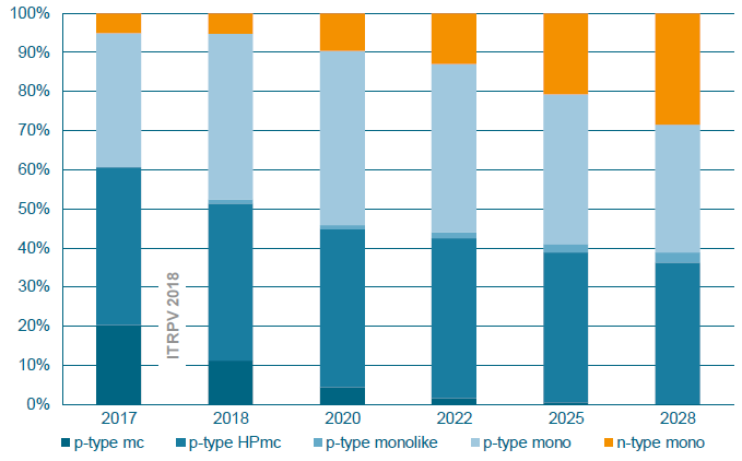
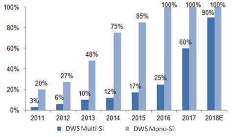
After China '531 New PV Policy', the domestic demand in 2018H2 plummeted, and the price of the entire PV industry chain fell sharply. For price and market share, there is always a tug of war between mono-si and multi-si. From the historical market share of mono-si and multi-si, although the market share of mono-si has been steadily increasing in recent years, multi-si has always occupied a higher market share. In 2017, multi-si products accounted for more than 60%. ITRPV2018 predicts that the market share of mono-si will continue to increase in 2018, and it is expected to be equal to multi-si.
In this context, it will be crucial for multi-si to remain competitive. In fact, the multi-si industry chain has been working to improve the price/performance ratio of products from ingots to sawing, cell and module, and there is still room for further improvement.

World market share of different wafer types
From: ITRPV 2018
Diamond wire sawing technology and development direction
In the silicon wafer field, the use of diamond wire sawing (DWS) is an effective way for reducing the cost. It has multiple advantages such as less silicon consumption, less damage, more throughput and lower energy consumption. Diamond wire cutting is first promoted and applied to mono-si, and popularized in 2016, which makes the cost difference between mono-si and multi-si shrink rapidly, thereby promotes the market share of mono-si.
Before 2016, due to the difficulty in texturing of DWS multi-si wafer, the multi-si wafer is mainly based on slurry sawing. In recent years, with the maturity of the texturing solution on DWS multi-si wafer surface, the application of DWS technology in multi-si has been greatly promoted, and it is expected to completely replace slurry sawing in 2018.

Progress of diamond wire sawing wafer market
From: ASIACHEM
'China DWS and Black Silicon Annual Report 2018'
The widespread use of diamond wire sawing on multi-si led to an explosive growth in the diamond wire demand in 2017, showing a 'difficult to find a wire' situation, which triggered the expansion of enterprises and the entry of more participants. According to statistics, the demand for the diamond wire before the “531 New Deal” is 3.5 million km/month, and the production capacity of the diamond wire is conservatively estimated at 8 million km/month. Currently, the demand has dropped to 1.5 million km/month, and the production capacity of the diamond wire is extremely oversupplied. Manufacturers with high cost and poor quality will be eliminated, and the diamond wire industry will change from 'difficult to find a wire' to 'price reduction and quality improvement'.
Therefore, the thinning of silicon wafer and the fining of diamond wire are imperative. By thinning and fining, silicon consumption reduced, the silicon wafer yield can be increased, that reduce the cost of diamond wire sawing. At present, the mainstream silicon wafer thickness is 180μm, and the leading wafer manufacturer has the technical capability of mass production of 150μm, and it is expected to drop to 140-100μm in the future. At present, the mainstream diameters of the diamond wire used to saw mono-si and multi-si are 60μm and 65μm, respectively, and it is expected to be reduced to 40μm and 50μm, respectively. It can be seen that the diamond wire sawing technology still has a large potential for cost reduction.
Current status and development direction of black silicon technology
In the silicon wafer part, the revolutionary diamond wire sawing multi-si technology demonstrates tremendous cost advantages. Aimed at the difficulty in texturing of DWS multi-si wafer, the industry has introduced a number of mature mass production solutions, including additives direct texturing technology, surface pretreatment technology and black silicon technology.
The biggest advantage of the additives direct texturing technology and surface pretreatment technology is that it does not need to increase the cost and is easy to realize mass production. Therefore, it has been applied to a certain scale in the early stage of the promotion of DWS multi-si, but this method doesn't improve the cell efficiency, which limits its further development; black silicon technology is divided into wet black silicon texturing technology and RIE technology, both of which can perfectly solve the problem of DWS multi-si wafer surface texture and have high efficiency gain, only RIE technology with higher investment in equipment than wet black silicon texturing technology, the latter can effectively improve cell efficiency with less investment, shows a higher cost performance.
According to statistics from ASIACHEM, the main producers of wet black silicon texturing include GCL, CSI, UNIEX PV, BYD, Suntech, and Risen, as of the first half of 2018, domestic black silicon texturing production capacity has reached 25GW. The wet black silicon process mainly uses Ag-containing additives, Cu/Ag and metal-free additive processes have a small number of applications; black silicon mass production machines are still mainly batch machines, and a small number of continuous machines are being evaluated.
The wet black silicon process is ushered in an important direction of cost reduction - single sided black silicon. Single-sided black silicon is the transformation of single-wafer loading and bifacial texturing in the production process into double-wafers loading and mono facial texturing. It is easy to upgrade from the existing equipment, and capacity increases by nearly 100%, the processing cost is reduced by more than 40%, and the amount of waste discharge is reduced by nearly 50% under the same throughput. It is reported that the production cost of single-sided black silicon can be reduced to ¥0.02-0.05/piece, the cost is almost equal to the traditional texturing process, and the efficiency gain can reach 0.3%-0.5%.

Single-sided black silicon texturing process
From: CSI
After the launch of the first generation of "TS" bifacial black silicon products, GCL-Poly launched the "TS+" series of single-sided black silicon wafers in November 2017. The product pioneered the unique process of 'front side texturing + rear side polishing', with excellent surface light trapping performance and better rear passivation effect, higher efficiency and lower cost, and significantly improved cost performance. Polishing technology is used on the rear side of “TS+”, which reduces the cost of wafer texturing process by more than 40% and is more suitable for PERC technology. Through a series of process optimizations, the cell efficiency gain of the "TS+" second-generation black silicon wafer will be increased to 0.5%, and the module power gain will be increased to 5W (60pcs). In 2018, the GCL-Poly Yangzhou base implemented a 5GW single-sided black silicon technology upgrade, and the "TS+" second-generation black silicon wafer also won the 2018SNEC highest-grade Taiwa Diamond Award.
'Diamond wire + black silicon + PERC': the only way for high-efficiency multi-si cell
As mentioned above, "Golden Wire + Wet Black Silicon" can increase the cell efficiency gain by 0.3-0.5% at a cost close to the traditional texturing. After superimposing the PERC technology, the cell efficiency of the black silicon PERC can be increased by 1.2-1.5%, and the average efficiency of mass production is 20.1%-20.4%. The efficiency gain of "Diamond wire + Black silicon + PERC" is still about 0.2-0.3% higher than the gain sum of ordinary multi black silicon and PERC, achieving the effect of "1+1>2", bringing a higher cost performance to the industry.
GCL in the 2018SENC released the ultra-efficient 300W+ series of new products, using the diamond wire high-efficiency black silicon PERC technology. Among them, the 300W+ single glass series MBB multi-si module with “TS+” second generation black silicon wafer is used, and the mass production power is up to 305W. It is the most effective multi module with conventional panel of the global mass production module, exceeding the application PV Leader's full score standard.
In addition, according to Dr. Qu Xiaohua, CEO of CSI, CSI will also mass produce "high-efficiency ingot + black silicon + PERC" ultra-efficient multi black silicon PERC technology in 2019, mass production cell efficiency is expected to reach 21.1%, Hope to achieve mono-si performance at multi-si cost and continue to enhance the competitiveness of multi-si products.
The diamond wire + black silicon combination technology has realized the efficiency increased and cost reduction of multi-si products, and there is still room for improvement. Coupled with PERC technology, it will undoubtedly make muliti-si products more cost-effective and competitive. As for the war between mono-si and multi-si, quoted from Dr. Qu Xiaohua, multi-si and mono-si, just like ebb and flow, each has its times. In the future, the market will give an answer.
3rd Diamond Wire Sawing and Black Silicon Technology Forum 2018 will be held on 12 Sep. in Changzhou, Jiangsu, China. Experts from GCL, CSI, Uniex, Suntech, Sumec, Nakamura, Gaoce Techology, Rietech, 1366 Technologies, Renesola, IMECAS, Nanchang University, IHS Markit, etc. will attend the forum and make wonderful presentations.